Journals > > Topics > Special Issue for Ultrafast Optics
Special Issue for Ultrafast Optics|33 Article(s)
Nanophotonic Methods for Chiral Sensing and Characterization(Invited)
Guanghao RUI, and Qiwen ZHAN
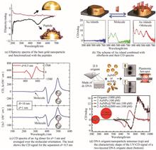
Chirality is a geometrical property where an object can not be superposed onto its mirror image via either a translational or a rotational operation. Since this type of symmetry is much harder to be maintained than to be broken, chirality exists widely in various macroscopic and microscopic structures. For example, proteins and nucleic acids are built of chiral amino acids and chiral sugar. In addition, DNA double helix, sugar, quartz, cholesteric liquid crystals and biomolecules are also chiral structures. Although molecules with different handedness have the same chemical construction, usually they would possess distinct chemical behaviors. Consequently, as an essential attribute of organism, the chiral representation of matter is of great significance in the fields of pharmacology, toxicology and pharmacodynamics. When electromagnetic wave interacts with chiral materials, special optical activity phenomena will appear, such as optical rotation, circular dichroism, and chiral optical force, which become a powerful tool for material chirality detection. Since the size of chiral molecule is much smaller than the wavelength of excitation light, the chiroptical effect of molecule itself is usually very weak, which greatly limits the accuracy of detection scheme. In recent years, the progress of nanophotonic technology is expected to enhance the weak chiral optical effect between light and matter at nanoscale, making it possible to detect chirality with high sensitivity and resolution. In this paper, the developments of chiral detection technology in recent years are reviewed, which focus on the micro/nano structure based enhanced circular dichroism and optical force effect. Besides, the corresponding applications are discussed. The mechanisms of chirality sensing for various nanophotonic platforms and outlined recent advances and future opportunities of major approaches for biosensing applications are reviewed. Firstly, the microscopic origin of surface-enhanced circular dichroism, as well as the theory of superchiral near-field generation in dielectric and plasmonic substrates are discussed. Secondly, the theory and mechanistic concept of plasmon-coupled circular dichroism in plasmonic nanoparticles, as well as the examples of hotspot-enhanced plasmon-coupled circular dichroism for biosensing applications are reviewed. Thirdly, the use of chiral and achiral plasmonic and dielectric nanoantennas, as well as plasmonic-dielectric hybrid systems for enhancing the optical chirality of biomolecules are reviewed. Fourthly, the theory of the optical force exerted on chiral nanoparticle is introduced. The optical sorting of chiral material with the use of the lateral optical force of complex optical field, the enhanced chiral optical force of plasmonic nanostructure, as well as the characterization of structured chirality using photoinduced force microscopy are reviewed. Finally, the future perspective of this rapidly developing field is presented at the end of this paper. Chirality is a geometrical property where an object can not be superposed onto its mirror image via either a translational or a rotational operation. Since this type of symmetry is much harder to be maintained than to be broken, chirality exists widely in various macroscopic and microscopic structures. For example, proteins and nucleic acids are built of chiral amino acids and chiral sugar. In addition, DNA double helix, sugar, quartz, cholesteric liquid crystals and biomolecules are also chiral structures. Although molecules with different handedness have the same chemical construction, usually they would possess distinct chemical behaviors. Consequently, as an essential attribute of organism, the chiral representation of matter is of great significance in the fields of pharmacology, toxicology and pharmacodynamics. When electromagnetic wave interacts with chiral materials, special optical activity phenomena will appear, such as optical rotation, circular dichroism, and chiral optical force, which become a powerful tool for material chirality detection. Since the size of chiral molecule is much smaller than the wavelength of excitation light, the chiroptical effect of molecule itself is usually very weak, which greatly limits the accuracy of detection scheme. In recent years, the progress of nanophotonic technology is expected to enhance the weak chiral optical effect between light and matter at nanoscale, making it possible to detect chirality with high sensitivity and resolution. In this paper, the developments of chiral detection technology in recent years are reviewed, which focus on the micro/nano structure based enhanced circular dichroism and optical force effect. Besides, the corresponding applications are discussed. The mechanisms of chirality sensing for various nanophotonic platforms and outlined recent advances and future opportunities of major approaches for biosensing applications are reviewed. Firstly, the microscopic origin of surface-enhanced circular dichroism, as well as the theory of superchiral near-field generation in dielectric and plasmonic substrates are discussed. Secondly, the theory and mechanistic concept of plasmon-coupled circular dichroism in plasmonic nanoparticles, as well as the examples of hotspot-enhanced plasmon-coupled circular dichroism for biosensing applications are reviewed. Thirdly, the use of chiral and achiral plasmonic and dielectric nanoantennas, as well as plasmonic-dielectric hybrid systems for enhancing the optical chirality of biomolecules are reviewed. Fourthly, the theory of the optical force exerted on chiral nanoparticle is introduced. The optical sorting of chiral material with the use of the lateral optical force of complex optical field, the enhanced chiral optical force of plasmonic nanostructure, as well as the characterization of structured chirality using photoinduced force microscopy are reviewed. Finally, the future perspective of this rapidly developing field is presented at the end of this paper.
Acta Photonica Sinica
- Publication Date: May. 25, 2022
- Vol. 51, Issue 5, 0551301 (2022)


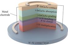
Effect of the Thickness of the a-Si Bonding Layer at InGaAs/Si Bonded Interface on the Performance of InGaAs/Si Avalanche Photodiode
Shixian SHE, Ye ZHANG, Zhiwei HUANG, Jinrong ZHOU, and Shaoying KE
Avalanche Photodiode (APD) is a popular device for the detection of light with low energy. It has been commonly used in LIDAR, quantum communication, deep space application, and remote sensing. In comparison to visible light detection, extending the spectral range of the APD into the short-wave infrared region (especially 1 310 nm and 1 550 nm) has a number of competitive advantages, such as high atmospheric transmission through smoke, smog, and fog, high compatibility with low-loss fiber communication, enhanced eye-safety threshold for free-space exploration, and low solar radiation background level for single-photon detection. The combination of InGaAs material and Si material is an ideal solution for the fabrication of high-performance APDs for the detection of weak light at communication band due to the fact that the absorption coefficient of InGaAs material is high at near-infrared range and Si material exhibits excellent avalanche characteristic thanks to the low electron/hole ionization coefficient ratio (0.02). However, due to the 7.7% lattice mismatch between InGaAs and Si, high-density threading dislocations form in Si-based epitaxial InGaAs film, leading to the high dark current and high noise in InGaAs/Si APD. While, high-quality Si-based InGaAs film can be achieved by InGaAs/Si hetero wafer bonding and layer exfoliation. The InP-based epitaxial InGaAs thin film is bonded to the Si-based epitaxial Si film by direct bonding method. This is a potential method for the fabrication of high-performance InGaAs/Si APD. However, the reported direct wafer bonding technique still cannot isolate the lattices of InGaAs and Si fundamentally due to the fact that the lattices of InGaAs and Si is directly contacted to each other during bonding, leading to the formation of misfit dislocations at the bonded interface. Thus, the lattices of InGaAs and Si materials should be segregated for the elimination of nucleation of dislocations. Using amorphous semiconductor intermediate layer, the lattice between InGaAs and Si can be isolated thoroughly. In addition, the quality of InGaAs absorption layer and Si multiplication layer, and good carrier transport at bonded interface can be ensured. However, the effect of a-Si material with high defect density and lager bandgap on the performance of InGaAs/Si APD has never been reported. In this paper, we first simulate the effect of the thickness of a-Si bonding layer on the performance of InGaAs/Si APD. Ultra-low dark current of the device is achieved at room temperature. Besides, when the bias is larger than breakdown voltage, a current gap appears between optical current and dark current. Extremely low dark current is achieved. This may give guidance for the fabrication of low-noise InGaAs/Si APD. Avalanche Photodiode (APD) is a popular device for the detection of light with low energy. It has been commonly used in LIDAR, quantum communication, deep space application, and remote sensing. In comparison to visible light detection, extending the spectral range of the APD into the short-wave infrared region (especially 1 310 nm and 1 550 nm) has a number of competitive advantages, such as high atmospheric transmission through smoke, smog, and fog, high compatibility with low-loss fiber communication, enhanced eye-safety threshold for free-space exploration, and low solar radiation background level for single-photon detection. The combination of InGaAs material and Si material is an ideal solution for the fabrication of high-performance APDs for the detection of weak light at communication band due to the fact that the absorption coefficient of InGaAs material is high at near-infrared range and Si material exhibits excellent avalanche characteristic thanks to the low electron/hole ionization coefficient ratio (0.02). However, due to the 7.7% lattice mismatch between InGaAs and Si, high-density threading dislocations form in Si-based epitaxial InGaAs film, leading to the high dark current and high noise in InGaAs/Si APD. While, high-quality Si-based InGaAs film can be achieved by InGaAs/Si hetero wafer bonding and layer exfoliation. The InP-based epitaxial InGaAs thin film is bonded to the Si-based epitaxial Si film by direct bonding method. This is a potential method for the fabrication of high-performance InGaAs/Si APD. However, the reported direct wafer bonding technique still cannot isolate the lattices of InGaAs and Si fundamentally due to the fact that the lattices of InGaAs and Si is directly contacted to each other during bonding, leading to the formation of misfit dislocations at the bonded interface. Thus, the lattices of InGaAs and Si materials should be segregated for the elimination of nucleation of dislocations. Using amorphous semiconductor intermediate layer, the lattice between InGaAs and Si can be isolated thoroughly. In addition, the quality of InGaAs absorption layer and Si multiplication layer, and good carrier transport at bonded interface can be ensured. However, the effect of a-Si material with high defect density and lager bandgap on the performance of InGaAs/Si APD has never been reported. In this paper, we first simulate the effect of the thickness of a-Si bonding layer on the performance of InGaAs/Si APD. Ultra-low dark current of the device is achieved at room temperature. Besides, when the bias is larger than breakdown voltage, a current gap appears between optical current and dark current. Extremely low dark current is achieved. This may give guidance for the fabrication of low-noise InGaAs/Si APD.
Acta Photonica Sinica
- Publication Date: Feb. 25, 2022
- Vol. 51, Issue 2, 0251218 (2022)
Passively Mode-locked Erbium-doped Fiber Laser Based on Nonlinear Fiber Loop Mirror
Zhaoyang ZHANG, Baole LU, Haowei CHEN, Kaige WANG, and Jintao BAI
In this paper, a passively mode-locked erbium-doped fiber laser with tunable wavelength of the "8" cavity based on a nonlinear fiber loop mirror is studied. The laser uses a 2×2 coupler with a coupling ratio of 30/70 to control a section of the laser with polarization controller. And a Sagnac ring is constructed at the right end of the entire resonant cavity to form a filter. When the pump power up to 270 mW, we tune the polarization controller to achieve a stable mode-locked state, the fiber laser outputs a traditional soliton with a center wavelength of 1 555.7 nm, the 3-dB bandwidth of the spectrum is 4.2 nm and the repetition frequency is 21.1 MHz, respectively. The results match the cavity length built in the experiment, the signal-to-noise ratio of the output laser is 68 dB, after fitting the autocorrelation curve of the output pulse, the pulse width is 0.759 ps, and the time bandwidth product is 0.397. Collecting the spectrum every 2 hours in the experiment, observe the changes with time of the two peaks of the left and right sidebands closest to the center wavelength in the spectrum and the change of the output power with time during the whole process, and analyze the results to calculate the output . The fluctuation of the power in the course of more than 20 hours is only 0.11 mW, which explain the excellent stability of this fiber laser. In addition, we only increase the pump power without moving other components in the cavity, due to the stress of the polarization controller, the single-mode fiber causes the internal unbalanced pressure of the fiber to introduce stress birefringence, and together with PC-2, which forms a filter with a smaller bandwidth and realizes the continuous tunable output of the mode-locked fiber laser. The tuning range of the wavelength interval is 1.5 nm. After increasing the pump power to 360 mW, we adjust the polarization controller to introduce excessive nonlinearity in the laser cavity, the soliton become unstable. Due to the peak power clamping effect, pulse splitting can occur and the modulation period of the spectrum is 0.467 nm. According to the relationship between the time domain spacing and the spectral spacing, the pulse spacing of the two sets of pulse output terminals is calculated to be about 17.23 ps. Further collect its autocorrelation graph, which can be seen from the autocorrelation graph. The pulse interval is obviously greater than 5 times the pulse width, so it is concluded that the fiber laser produces a bound state soliton at this time, and it is in a loosely bound state. The mode-locking threshold of this laser is 270 mW at the pump power is 5.67 mW. From 270 mW to 360 mW, the overall mode-locked output power increases linearly, and the overall output power slope is 2.42%. The low light-to-light conversion efficiency is caused by the loss of the fiber fusion splice in the cavity. The fiber laser has a simple structure, easy tuning and has good stability. It provides a technical method for realizing wavelength tuning and traditional soliton mode locking, it can also be used as a seed light source in optical communications. In this paper, a passively mode-locked erbium-doped fiber laser with tunable wavelength of the "8" cavity based on a nonlinear fiber loop mirror is studied. The laser uses a 2×2 coupler with a coupling ratio of 30/70 to control a section of the laser with polarization controller. And a Sagnac ring is constructed at the right end of the entire resonant cavity to form a filter. When the pump power up to 270 mW, we tune the polarization controller to achieve a stable mode-locked state, the fiber laser outputs a traditional soliton with a center wavelength of 1 555.7 nm, the 3-dB bandwidth of the spectrum is 4.2 nm and the repetition frequency is 21.1 MHz, respectively. The results match the cavity length built in the experiment, the signal-to-noise ratio of the output laser is 68 dB, after fitting the autocorrelation curve of the output pulse, the pulse width is 0.759 ps, and the time bandwidth product is 0.397. Collecting the spectrum every 2 hours in the experiment, observe the changes with time of the two peaks of the left and right sidebands closest to the center wavelength in the spectrum and the change of the output power with time during the whole process, and analyze the results to calculate the output . The fluctuation of the power in the course of more than 20 hours is only 0.11 mW, which explain the excellent stability of this fiber laser. In addition, we only increase the pump power without moving other components in the cavity, due to the stress of the polarization controller, the single-mode fiber causes the internal unbalanced pressure of the fiber to introduce stress birefringence, and together with PC-2, which forms a filter with a smaller bandwidth and realizes the continuous tunable output of the mode-locked fiber laser. The tuning range of the wavelength interval is 1.5 nm. After increasing the pump power to 360 mW, we adjust the polarization controller to introduce excessive nonlinearity in the laser cavity, the soliton become unstable. Due to the peak power clamping effect, pulse splitting can occur and the modulation period of the spectrum is 0.467 nm. According to the relationship between the time domain spacing and the spectral spacing, the pulse spacing of the two sets of pulse output terminals is calculated to be about 17.23 ps. Further collect its autocorrelation graph, which can be seen from the autocorrelation graph. The pulse interval is obviously greater than 5 times the pulse width, so it is concluded that the fiber laser produces a bound state soliton at this time, and it is in a loosely bound state. The mode-locking threshold of this laser is 270 mW at the pump power is 5.67 mW. From 270 mW to 360 mW, the overall mode-locked output power increases linearly, and the overall output power slope is 2.42%. The low light-to-light conversion efficiency is caused by the loss of the fiber fusion splice in the cavity. The fiber laser has a simple structure, easy tuning and has good stability. It provides a technical method for realizing wavelength tuning and traditional soliton mode locking, it can also be used as a seed light source in optical communications.
Acta Photonica Sinica
- Publication Date: Feb. 25, 2022
- Vol. 51, Issue 2, 0251217 (2022)
Preparation and Performance of g-C3N4/Bi2S3 Composite Broad-band Photodetector
Xiangming FANG, Ping RONG, Shuai REN, Zhaoyang WANG, Shiyong GAO, and Jinzhong WANG
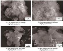
Broad-band Photodetectors (PDs) become a foucus of current research due to extensive use in missiles guidance, flame monitoring, chemical analysis, biomedical imaging, optical communication and so on. The PDs based on semiconductors, in particular, attach much attention in trerms of their fast response speed, high sensitivity, small volume and weight. Thereinto, the g-C3N4 nanomaterial is proven to possess many benefits for application to PDs such as the unique electronic structure, excellent thermal and chemical properties, non-toxic and raw material sufficient. For further broading the optical detection range and improving the detection performance of the g-C3N4 PD, coupling g-C3N4 and Bi2S3 nanomaterial with a narrow bandgap of 1.3 eV is probably an effective strategy. However, there are few reports on the research of g-C3N4/Bi2S3 composite for PDs. In this study, g-C3N4 and Bi2S3 nanomaterials have been prepared using thermal polymerization method and g-C3N4/Bi2S3 composite structure has been further synthesized with the solution method. The surface morphology of the samples have been characterized through scanning electron microscope. And the results suggest that Bi2S3 particales are attached to g-C3N4 nanosheets, and the layered structure of g-C3N4 is not broken after composited with Bi2S3. The X-ray diffractometer has been used to analyze the crystalline structure of the as-synthesized g-C3N4/Bi2S3 composite. It can be clearly seen that the g-C3N4/Bi2S3 composite has great crystal quality. In addition, the PD based on g-C3N4/Bi2S3 composite structure has been preapred. Under ultraviolet (UV) light illumination, it is indicated that the detection performance of the g-C3N4/Bi2S3 PD for UV light is significantly improved, and its maximum photocurrent is as high as 12.93 μA, which is about 12 times than that of g-C3N4 PD. Meanwhile, the g-C3N4/Bi2S3 PD also exhibits excellent stability and reproductivity, as well as the fast response rise time of 30.36 ms and decay time of 25.56 ms. When exposed to green light at wavelength of 530 nm, the maximum photocurrent of g-C3N4/Bi2S3 PD after 10 times of recycle still remaines steady at about 9.5 μA. Upon irradiation with a red light of wavelength 625 nm, the g-C3N4/Bi2S3 PD also can reach the maximum value (7.6 μA) and then remain stable. Obviously, the g-C3N4/Bi2S3 PD has well photoresponse characteristic and stability compared with the g-C3N4 PD in the visible(Vis) light region, which shows broad-band detection characteristic. What is more, a possible mechanism of UV/Vis detection of the g-C3N4/Bi2S3 PD has been proposed. Apparently, the enhanced detection performance of g-C3N4/Bi2S3 PD is attributed to the formation heterojunction between g-C3N4 and Bi2S3, which refrains the recombination of photogenerated carriers and promotes the efficiency seperation of charges. Besides, the Bi2S3 is a typical narrow bandgap semiconductor, broading the detecton range of g-C3N4/Bi2S3 PD from the UV to Vis region. In view of the excellent performance of the g-C3N4/Bi2S3 composite, the g-C3N4/Bi2S3 is expected to be widely applied in diverse applications, such as photocatalysis, sensors and solar cell, etc. Broad-band Photodetectors (PDs) become a foucus of current research due to extensive use in missiles guidance, flame monitoring, chemical analysis, biomedical imaging, optical communication and so on. The PDs based on semiconductors, in particular, attach much attention in trerms of their fast response speed, high sensitivity, small volume and weight. Thereinto, the g-C3N4 nanomaterial is proven to possess many benefits for application to PDs such as the unique electronic structure, excellent thermal and chemical properties, non-toxic and raw material sufficient. For further broading the optical detection range and improving the detection performance of the g-C3N4 PD, coupling g-C3N4 and Bi2S3 nanomaterial with a narrow bandgap of 1.3 eV is probably an effective strategy. However, there are few reports on the research of g-C3N4/Bi2S3 composite for PDs. In this study, g-C3N4 and Bi2S3 nanomaterials have been prepared using thermal polymerization method and g-C3N4/Bi2S3 composite structure has been further synthesized with the solution method. The surface morphology of the samples have been characterized through scanning electron microscope. And the results suggest that Bi2S3 particales are attached to g-C3N4 nanosheets, and the layered structure of g-C3N4 is not broken after composited with Bi2S3. The X-ray diffractometer has been used to analyze the crystalline structure of the as-synthesized g-C3N4/Bi2S3 composite. It can be clearly seen that the g-C3N4/Bi2S3 composite has great crystal quality. In addition, the PD based on g-C3N4/Bi2S3 composite structure has been preapred. Under ultraviolet (UV) light illumination, it is indicated that the detection performance of the g-C3N4/Bi2S3 PD for UV light is significantly improved, and its maximum photocurrent is as high as 12.93 μA, which is about 12 times than that of g-C3N4 PD. Meanwhile, the g-C3N4/Bi2S3 PD also exhibits excellent stability and reproductivity, as well as the fast response rise time of 30.36 ms and decay time of 25.56 ms. When exposed to green light at wavelength of 530 nm, the maximum photocurrent of g-C3N4/Bi2S3 PD after 10 times of recycle still remaines steady at about 9.5 μA. Upon irradiation with a red light of wavelength 625 nm, the g-C3N4/Bi2S3 PD also can reach the maximum value (7.6 μA) and then remain stable. Obviously, the g-C3N4/Bi2S3 PD has well photoresponse characteristic and stability compared with the g-C3N4 PD in the visible(Vis) light region, which shows broad-band detection characteristic. What is more, a possible mechanism of UV/Vis detection of the g-C3N4/Bi2S3 PD has been proposed. Apparently, the enhanced detection performance of g-C3N4/Bi2S3 PD is attributed to the formation heterojunction between g-C3N4 and Bi2S3, which refrains the recombination of photogenerated carriers and promotes the efficiency seperation of charges. Besides, the Bi2S3 is a typical narrow bandgap semiconductor, broading the detecton range of g-C3N4/Bi2S3 PD from the UV to Vis region. In view of the excellent performance of the g-C3N4/Bi2S3 composite, the g-C3N4/Bi2S3 is expected to be widely applied in diverse applications, such as photocatalysis, sensors and solar cell, etc.
Acta Photonica Sinica
- Publication Date: Feb. 25, 2022
- Vol. 51, Issue 2, 0251216 (2022)
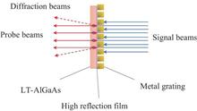
Experimental Study on the Spatial Performance of Photorefractive X-ray Semiconductor Ultrafast Response Chip
Xiaobo TAN, Xin YAN, Tao YI, Kai HE, Zhengzheng SHAO, Kaikai ZHOU, Guilong GAO, Tao WANG, Jun ZHANG, and Zhaowen ZHUANG
The traditional ultrafast electric vacuum devices are usually based on the mechanism of photoelectric conversion, and their performance is restricted by factors such as material response and space-charge effect. It is difficult for the devices like microchannel plate framing cameras, DIlation X-ray Imager (DIXI), streak cameras to achieve high temporal resolution (100 fs~1 ps) and spatial resolution (~μm) two-dimensional imaging. Ultrafast imaging technology based on photorefractive effect is a new ultrafast diagnostic technology, which has the advantages of high spatiotemporal resolution, all-optical, all-solid-state, and anti-radiation. The nonequilibrium carrier lifetime of low-temperature grown AlGaAs (LT-AlGaAs) can reach ps-level. The Ultrafast Response Chip (URC) made of LT-AlGaAs has the characteristics of high temporal resolution, meanwhile, good spatial performance is the other key factor for its application. In this paper, the spatial performance of LT-AlGaAs URC is experimentally studied using X-ray, generated by high-energy nanosecond pulsed laser-produced plasma, as the signal. The results show that the URC has the ability of high spatial resolution and large-scale imaging in the X-ray energy dynamic range of 120∶1. The optimal spatial resolution is ≥ 35 lp/mm @ MTF = 0.1, and the imaging frame can reach 6.7 mm × 6.7 mm. The results further verify the feasibility of ultrafast diagnostic technology based on photorefractive materials. In the future, LT-AlGaAs URC will be combined with ultrafast framing technologies such as dispersion framing and polarization chirp framing to realize multi-frames and high spatiotemporal resolution two-dimensional imaging. The traditional ultrafast electric vacuum devices are usually based on the mechanism of photoelectric conversion, and their performance is restricted by factors such as material response and space-charge effect. It is difficult for the devices like microchannel plate framing cameras, DIlation X-ray Imager (DIXI), streak cameras to achieve high temporal resolution (100 fs~1 ps) and spatial resolution (~μm) two-dimensional imaging. Ultrafast imaging technology based on photorefractive effect is a new ultrafast diagnostic technology, which has the advantages of high spatiotemporal resolution, all-optical, all-solid-state, and anti-radiation. The nonequilibrium carrier lifetime of low-temperature grown AlGaAs (LT-AlGaAs) can reach ps-level. The Ultrafast Response Chip (URC) made of LT-AlGaAs has the characteristics of high temporal resolution, meanwhile, good spatial performance is the other key factor for its application. In this paper, the spatial performance of LT-AlGaAs URC is experimentally studied using X-ray, generated by high-energy nanosecond pulsed laser-produced plasma, as the signal. The results show that the URC has the ability of high spatial resolution and large-scale imaging in the X-ray energy dynamic range of 120∶1. The optimal spatial resolution is ≥ 35 lp/mm @ MTF = 0.1, and the imaging frame can reach 6.7 mm × 6.7 mm. The results further verify the feasibility of ultrafast diagnostic technology based on photorefractive materials. In the future, LT-AlGaAs URC will be combined with ultrafast framing technologies such as dispersion framing and polarization chirp framing to realize multi-frames and high spatiotemporal resolution two-dimensional imaging.
Acta Photonica Sinica
- Publication Date: Feb. 25, 2022
- Vol. 51, Issue 2, 0251215 (2022)

Fabrication and Photoresponse Study of the Photodetector Based on Novel NiO-Bi2Te3 Heterostructure
Minggang SHI, Haichuan MU, and Min QIAN
As a significant p-type semiconductor, NiO is widely studied for its gas sensing and electrochromism characteristics, whereas researches concerning its photodetection properties are rarely reported. Herein, we fabricated a photodetector based on NiO/Bi2Te3 heterostructure and studied the influence of NiO’s concentrations as well as the Localized Surface Plasmon Resonance (LSPR) effect of the Au NPs on the device’s photoresponse.For the device fabrication, NiO film was spin-coated on the FTO glass, followed by baking and annealing to form high quality crystal film. Then, Chemical Vapor Deposition (CVD) method was adopted to lay Bi2Te3 nanoplates on the NiO film, forming the NiO-Bi2Te3 heterostructure. Finally, the device was achieved via photolithographic process and Ag electrodes deposition, featuring a vertical structure with FTO working as the anode and Ag serving as the cathode.X-Ray Diffraction (XRD) and Scanning Electron Microscope (SEM) results demonstrate the favorable crystal quality of NiO film and Bi2Te3 nanoplates. Energy Dispersive Spectrometer (EDS) image manifests the uniform distribution of different elements and Photoluminescence (PL) spectra were applied to study the mechanism of electron-hole separation. All these results could be condensed to the point that the NiO film with the concentration of 0.5 mol/L shows the optimal crystal quality and the doping of Au NPs aids the separation of electron-hole pairs. Furthermore, we also performed photo-electric tests to evaluate the influence of the NiO concentration and the results show that the device achieves optimal response with the concentration of NiO fixed at 0.5 mol/L, which meshes well with the characterizing results.In addition, tests regarding photoresponse to wavelength, power density and on/off switching were conducted in ambient environment. With the presence of Au NPs, the maximum responsivity (R) of the device reaches 1236 mA/W, about 21% higher compared to that of the pristine NiO, owing to the boosted light absorption caused by the LSPR effect of Au NPs. To elucidate the weak signal detecting ability, the specific detectivity (D*) of the device is calculated and it attains the value of 5.97×10¹⁰ Jones. Besides, the photo gain exceeds 400%, indicating that there are more than 4 photoexcited carriers generated by per absorbed photon. Beyond that, the formation of Schottky contact between NiO and Au NPs will facilitate the separation of electron-hole pairs, thus accelerating the response process and shrinking the rise time (Tr) and decay time (Td) to 92 ms and 62 ms, respectively. The study corroborates the enhancement of photoresponse resulted from the two internal electrical field due to the introduction of NiO/Bi2Te3 junction and Au/NiO Schottky junction as well as the LSPR effect from Au NPs.This research offers a feasible approach for the realization of NiO-based photodetector and sheds light on the enormous potential of the NiO's application in photodetection. As a significant p-type semiconductor, NiO is widely studied for its gas sensing and electrochromism characteristics, whereas researches concerning its photodetection properties are rarely reported. Herein, we fabricated a photodetector based on NiO/Bi2Te3 heterostructure and studied the influence of NiO’s concentrations as well as the Localized Surface Plasmon Resonance (LSPR) effect of the Au NPs on the device’s photoresponse.For the device fabrication, NiO film was spin-coated on the FTO glass, followed by baking and annealing to form high quality crystal film. Then, Chemical Vapor Deposition (CVD) method was adopted to lay Bi2Te3 nanoplates on the NiO film, forming the NiO-Bi2Te3 heterostructure. Finally, the device was achieved via photolithographic process and Ag electrodes deposition, featuring a vertical structure with FTO working as the anode and Ag serving as the cathode.X-Ray Diffraction (XRD) and Scanning Electron Microscope (SEM) results demonstrate the favorable crystal quality of NiO film and Bi2Te3 nanoplates. Energy Dispersive Spectrometer (EDS) image manifests the uniform distribution of different elements and Photoluminescence (PL) spectra were applied to study the mechanism of electron-hole separation. All these results could be condensed to the point that the NiO film with the concentration of 0.5 mol/L shows the optimal crystal quality and the doping of Au NPs aids the separation of electron-hole pairs. Furthermore, we also performed photo-electric tests to evaluate the influence of the NiO concentration and the results show that the device achieves optimal response with the concentration of NiO fixed at 0.5 mol/L, which meshes well with the characterizing results.In addition, tests regarding photoresponse to wavelength, power density and on/off switching were conducted in ambient environment. With the presence of Au NPs, the maximum responsivity (R) of the device reaches 1236 mA/W, about 21% higher compared to that of the pristine NiO, owing to the boosted light absorption caused by the LSPR effect of Au NPs. To elucidate the weak signal detecting ability, the specific detectivity (D*) of the device is calculated and it attains the value of 5.97×10¹⁰ Jones. Besides, the photo gain exceeds 400%, indicating that there are more than 4 photoexcited carriers generated by per absorbed photon. Beyond that, the formation of Schottky contact between NiO and Au NPs will facilitate the separation of electron-hole pairs, thus accelerating the response process and shrinking the rise time (Tr) and decay time (Td) to 92 ms and 62 ms, respectively. The study corroborates the enhancement of photoresponse resulted from the two internal electrical field due to the introduction of NiO/Bi2Te3 junction and Au/NiO Schottky junction as well as the LSPR effect from Au NPs.This research offers a feasible approach for the realization of NiO-based photodetector and sheds light on the enormous potential of the NiO's application in photodetection.
Acta Photonica Sinica
- Publication Date: Feb. 25, 2022
- Vol. 51, Issue 2, 0251214 (2022)
Finite Element Thermal Analysis of Optical Lenses in 10 kW Rectangular Spot Laser Space Combiner
Ben LI, Jingfeng ZHOU, Yi WANG, and Yang BAI
A space-transmission high-power near-infrared semiconductor laser beam with a rectangular laser spot is one of the key tools to improve the efficiency and quality of laser surface heat treatment. However, this kind of laser is difficult to apply to the surface heat treatment of flexible lasers inside workpieces. This is because the volume of the lasers increases greatly with increasing laser power and is affected by the space transmission of the laser beam. The spot of the ultrahigh-power laser beam from a commercial high-power fiber laser or a fiber-transmitted semiconductor laser is circular, which makes it difficult to control the spot overlap rate during the laser surface heat treatment process. It is difficult to change the ultrahigh-power circular laser spot into a rectangular spot through beam shaping technology. Laser incoherent spatial combining based on multifiber transmission is an effective method to reduce the risk of high-power laser transmission in a single fiber and realize the flexible transmission of high-power lasers. It has quickly become a research hotspot in the field of ultrahigh power laser systems. To solve the spot overlap rate control problem of ultrahigh power lasers transmitted by fibers in flexible laser surface heat treatment, a design scheme of arranging 18 semiconductor laser beams at 972 nm transmitted by fibers according to a “staggered rectangle” and implementing space incoherent beam combination was proposed in this paper. Based on this, a set of 10 kW rectangular spot laser beam combiners was developed. The optical elements in the combiner are all optical lenses made of fused silica glass. It is widely known that the accumulation of heat generated by long-term ultrahigh-power laser beam irradiation will produce serious thermal effects inside the optical lens, resulting in reduced beam quality and even irreversible damage inside the optical lens, which will seriously affect the safety and reliability of the combiner for long-term operation. However, the structural shielding of the combiner often makes the thermodynamic properties of the optical lenses difficult to directly detect and evaluate with experimental methods. With the rapid development of computer technology and calculation methods, the establishment of temperature field models based on finite element analysis has become a simulation method widely used in the reliability analysis of laser irradiation optical components. At present, most thermodynamic finite element analysis studies on laser irradiation optical elements simplify the laser beam to an area heat source while ignoring the volume absorption of the laser beam by the optical element. However, the volume absorption of the laser beam by the optical lens itself is already one of the main factors affecting its thermodynamic properties with the continuous increase in laser incoherent space combining power. There is no report on the thermodynamic finite element analysis of multiple ultrahigh power laser beams transmitted through optical lenses under the premise that the laser beam is used as a volume heat source. To solve the above problems, the finite element thermodynamic model of the optical lens was established based on the mathematical model of the whole heat source of the 18 laser beams. The thermodynamic properties of all optical lenses under the condition of being irradiated by 18 laser beams participating in the combination for 1 000 s are simulated and analyzed using this model. The research results show that the maximum temperature, maximum thermal deformation and maximum equivalent thermal stress of the optical lens in the combiner stabilized after the 800 s time node. The simulated values of the maximum core temperature and the maximum equivalent thermal stress were 427.27 K and 12.68 MPa, respectively, which were significantly lower than the softening point temperature and thermal damage threshold of fused silica glass used to manufacture optical lenses. The maximum aperture of 0.1 corresponding to the simulated maximum thermal deformation of 4.53 μm was much smaller than the conventional machining tolerance of 2.0. The highest temperature on the exit surface of the window lens was measured during the laser beam combining time of 1 000 s. Both the experimental value and the simulated value of the highest temperature showed good consistency with the laser beam combining time. This shows that the established finite element thermal analysis model has good accuracy. The maximum combined power of 10.64 kW for the combined laser with a rectangular spot was measured when it was continuously operated for 1 000 s. The power instability of less than ±1.2% further experimentally verified the safety and reliability of the combiner under long-term operation. A space-transmission high-power near-infrared semiconductor laser beam with a rectangular laser spot is one of the key tools to improve the efficiency and quality of laser surface heat treatment. However, this kind of laser is difficult to apply to the surface heat treatment of flexible lasers inside workpieces. This is because the volume of the lasers increases greatly with increasing laser power and is affected by the space transmission of the laser beam. The spot of the ultrahigh-power laser beam from a commercial high-power fiber laser or a fiber-transmitted semiconductor laser is circular, which makes it difficult to control the spot overlap rate during the laser surface heat treatment process. It is difficult to change the ultrahigh-power circular laser spot into a rectangular spot through beam shaping technology. Laser incoherent spatial combining based on multifiber transmission is an effective method to reduce the risk of high-power laser transmission in a single fiber and realize the flexible transmission of high-power lasers. It has quickly become a research hotspot in the field of ultrahigh power laser systems. To solve the spot overlap rate control problem of ultrahigh power lasers transmitted by fibers in flexible laser surface heat treatment, a design scheme of arranging 18 semiconductor laser beams at 972 nm transmitted by fibers according to a “staggered rectangle” and implementing space incoherent beam combination was proposed in this paper. Based on this, a set of 10 kW rectangular spot laser beam combiners was developed. The optical elements in the combiner are all optical lenses made of fused silica glass. It is widely known that the accumulation of heat generated by long-term ultrahigh-power laser beam irradiation will produce serious thermal effects inside the optical lens, resulting in reduced beam quality and even irreversible damage inside the optical lens, which will seriously affect the safety and reliability of the combiner for long-term operation. However, the structural shielding of the combiner often makes the thermodynamic properties of the optical lenses difficult to directly detect and evaluate with experimental methods. With the rapid development of computer technology and calculation methods, the establishment of temperature field models based on finite element analysis has become a simulation method widely used in the reliability analysis of laser irradiation optical components. At present, most thermodynamic finite element analysis studies on laser irradiation optical elements simplify the laser beam to an area heat source while ignoring the volume absorption of the laser beam by the optical element. However, the volume absorption of the laser beam by the optical lens itself is already one of the main factors affecting its thermodynamic properties with the continuous increase in laser incoherent space combining power. There is no report on the thermodynamic finite element analysis of multiple ultrahigh power laser beams transmitted through optical lenses under the premise that the laser beam is used as a volume heat source. To solve the above problems, the finite element thermodynamic model of the optical lens was established based on the mathematical model of the whole heat source of the 18 laser beams. The thermodynamic properties of all optical lenses under the condition of being irradiated by 18 laser beams participating in the combination for 1 000 s are simulated and analyzed using this model. The research results show that the maximum temperature, maximum thermal deformation and maximum equivalent thermal stress of the optical lens in the combiner stabilized after the 800 s time node. The simulated values of the maximum core temperature and the maximum equivalent thermal stress were 427.27 K and 12.68 MPa, respectively, which were significantly lower than the softening point temperature and thermal damage threshold of fused silica glass used to manufacture optical lenses. The maximum aperture of 0.1 corresponding to the simulated maximum thermal deformation of 4.53 μm was much smaller than the conventional machining tolerance of 2.0. The highest temperature on the exit surface of the window lens was measured during the laser beam combining time of 1 000 s. Both the experimental value and the simulated value of the highest temperature showed good consistency with the laser beam combining time. This shows that the established finite element thermal analysis model has good accuracy. The maximum combined power of 10.64 kW for the combined laser with a rectangular spot was measured when it was continuously operated for 1 000 s. The power instability of less than ±1.2% further experimentally verified the safety and reliability of the combiner under long-term operation.
Acta Photonica Sinica
- Publication Date: Feb. 25, 2022
- Vol. 51, Issue 2, 0251213 (2022)
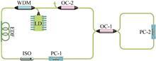
Generation of Stretched Pulse with Hundred-femtosecond Pulse Widths Based on Multimode-fiber Interference Effect
Mengru SUN, Haiying JI, Hao XIONG, Yao HONG, Wanzhuo MA, and Tianshu WANG
Ultrashort pulse fiber lasers have received widespread attention because they play a vital role in telecommunications, biology, and photonics. Many mode-locking technologies have been applied to construct passive mode-locking fiber lasers, such as semiconductor saturable absorption mirrors, graphene, nonlinear polarization rotation, carbon nanotubes, etc. In recent years, researchers have conducted extensive research on multimode fibers and proposed nonlinear multimode interference technology based on multimode fibers for the generation of ultrashort pulses. Compared with traditional mode-locked devices, multi-mode interference-based mode-locked devices have the advantages of high damage threshold, simple structure, adjustable wavelength and controllable modulation depth. In this study, we constructed a multimode interference mode-locked fiber laser by squeezing a piece of GIMF into the polarization controller works as SA. By introducing the dispersion management into the cavity, stretched pulse with 3 dB bandwidth of 37.2 nm was obtained. After compression, these pulses have a hundred-femtosecond duration. By carefully adjusting the PC and increasing the pump power, dispersion-managed soliton molecules was acquired, and the modulation period of spectrum is 0.32 nm. The experimental setup of the dispersion-managed all-fiber laser based on the SMS structure is depicted in Fig. 1. A 0.8 m long piece of single-mode HEDF was utilized as the gain medium, which was pumped by two 980 nm LDs through 980/1 550 nm WDM. Unidirectional operation was ensured by polarization independent optical isolator. The SA based on the SMS structure in the cavity was used as a mode-locking device, in which a 0.153 m long piece of GIMF was squeezed in the PC and the polarization states of the light in the multimode fiber was changed by tuning the PC. The net cavity dispersion can be managed by using a segment of DCF. In the experiment, the length of DCF is 0.3 m. The GVDs of HEDF, SMF, and DCF at 1.5 μm are 15.7, 18, and -?152.6 ps/nm·km, respectively. Due to the short length of the GIMF, the dispersion effect of the GIMF was neglected. Thus, the total net cavity dispersion is calculated to be -?0.105 09 ps2, and the laser operated in negative dispersion region. Considering the pigtails of all intracavity devices, the cavity length is 7.4 m, corresponding to the fundamental repetition frequency of 27.02 MHz. A 10∶90 OC was employed to collect 10% power from the cavity. A compressed structure was built to acquire the minimum pulse width. In order to avoid the splitting and distortion of the pulse caused by the excessive peak power during the power amplification process, a section of DCF was welded between the PC and the amplifier to stretch the pulse in advance. As the gain medium of the amplifying structure, the EDF with normal dispersion at 1 550 nm was also used as a part of dispersion compensation. The dispersion caused by the amplifier further reduced the chirp of the pulse. When the pump 1 and pump 2 increased to 95.1 mW and 350 mW, self-starting dispersion-managed mode-locked pulse can be observed by appropriately rotating and squeezing the GIMF inside the PC. Figure 3 shows the features of the SP with pump 1 and pump 2 power of 95.1 mW and 750 mW. As the pump power increased, the spectral bandwidth and output power became wider and bigger and arrived its maximum of 37.2 nm and 1.7 mW respectively. Optimizing the length of DCF can compress the pulse from 973.2 fs to 280.1fs with the compressed structure after the output port of cavity. When the pump 2 increased to 856 mW, the pulses form stable soliton molecules by carefully adjusting the PC. The pulse width of a single dispersion-managed soliton molecules is 4.04 ps, and the pulse interval is 24.1 ps, which corresponds to the 0.32 nm spectral modulation period. The output characteristics of stretched pulses and dispersion-managed soliton molecules in dispersion-managed multimode interference mode-locked fiber lasers are studied. The output of the mode-locked pulse is realized by squeezing the graded index multimode fiber into the polarization controller. When the total pump power is 845.1 mW, a stretched pulse with a central wavelength of 1 528 nm, a 3 dB bandwidth of 37.2 nm and a pulse width of 973.2 fs is obtained by carefully adjusting the PC. A compressor is built to acquire the minimum pulse width and the DCF is used for dispersion compensation to compress the pulse width of the stretched pulse to 280.1 fs. By further increasing the total pump power to 951.1 mW and adjusting the PC, the soliton molecules are obtained, and the modulation period of the dispersion-managed soliton molecules is 0.32 nm, corresponding to pulse interval of 24.1 ps. This phenomenon provides a reference for the research on multimode interference fiber lasers. Ultrashort pulse fiber lasers have received widespread attention because they play a vital role in telecommunications, biology, and photonics. Many mode-locking technologies have been applied to construct passive mode-locking fiber lasers, such as semiconductor saturable absorption mirrors, graphene, nonlinear polarization rotation, carbon nanotubes, etc. In recent years, researchers have conducted extensive research on multimode fibers and proposed nonlinear multimode interference technology based on multimode fibers for the generation of ultrashort pulses. Compared with traditional mode-locked devices, multi-mode interference-based mode-locked devices have the advantages of high damage threshold, simple structure, adjustable wavelength and controllable modulation depth. In this study, we constructed a multimode interference mode-locked fiber laser by squeezing a piece of GIMF into the polarization controller works as SA. By introducing the dispersion management into the cavity, stretched pulse with 3 dB bandwidth of 37.2 nm was obtained. After compression, these pulses have a hundred-femtosecond duration. By carefully adjusting the PC and increasing the pump power, dispersion-managed soliton molecules was acquired, and the modulation period of spectrum is 0.32 nm. The experimental setup of the dispersion-managed all-fiber laser based on the SMS structure is depicted in Fig. 1. A 0.8 m long piece of single-mode HEDF was utilized as the gain medium, which was pumped by two 980 nm LDs through 980/1 550 nm WDM. Unidirectional operation was ensured by polarization independent optical isolator. The SA based on the SMS structure in the cavity was used as a mode-locking device, in which a 0.153 m long piece of GIMF was squeezed in the PC and the polarization states of the light in the multimode fiber was changed by tuning the PC. The net cavity dispersion can be managed by using a segment of DCF. In the experiment, the length of DCF is 0.3 m. The GVDs of HEDF, SMF, and DCF at 1.5 μm are 15.7, 18, and -?152.6 ps/nm·km, respectively. Due to the short length of the GIMF, the dispersion effect of the GIMF was neglected. Thus, the total net cavity dispersion is calculated to be -?0.105 09 ps2, and the laser operated in negative dispersion region. Considering the pigtails of all intracavity devices, the cavity length is 7.4 m, corresponding to the fundamental repetition frequency of 27.02 MHz. A 10∶90 OC was employed to collect 10% power from the cavity. A compressed structure was built to acquire the minimum pulse width. In order to avoid the splitting and distortion of the pulse caused by the excessive peak power during the power amplification process, a section of DCF was welded between the PC and the amplifier to stretch the pulse in advance. As the gain medium of the amplifying structure, the EDF with normal dispersion at 1 550 nm was also used as a part of dispersion compensation. The dispersion caused by the amplifier further reduced the chirp of the pulse. When the pump 1 and pump 2 increased to 95.1 mW and 350 mW, self-starting dispersion-managed mode-locked pulse can be observed by appropriately rotating and squeezing the GIMF inside the PC. Figure 3 shows the features of the SP with pump 1 and pump 2 power of 95.1 mW and 750 mW. As the pump power increased, the spectral bandwidth and output power became wider and bigger and arrived its maximum of 37.2 nm and 1.7 mW respectively. Optimizing the length of DCF can compress the pulse from 973.2 fs to 280.1fs with the compressed structure after the output port of cavity. When the pump 2 increased to 856 mW, the pulses form stable soliton molecules by carefully adjusting the PC. The pulse width of a single dispersion-managed soliton molecules is 4.04 ps, and the pulse interval is 24.1 ps, which corresponds to the 0.32 nm spectral modulation period. The output characteristics of stretched pulses and dispersion-managed soliton molecules in dispersion-managed multimode interference mode-locked fiber lasers are studied. The output of the mode-locked pulse is realized by squeezing the graded index multimode fiber into the polarization controller. When the total pump power is 845.1 mW, a stretched pulse with a central wavelength of 1 528 nm, a 3 dB bandwidth of 37.2 nm and a pulse width of 973.2 fs is obtained by carefully adjusting the PC. A compressor is built to acquire the minimum pulse width and the DCF is used for dispersion compensation to compress the pulse width of the stretched pulse to 280.1 fs. By further increasing the total pump power to 951.1 mW and adjusting the PC, the soliton molecules are obtained, and the modulation period of the dispersion-managed soliton molecules is 0.32 nm, corresponding to pulse interval of 24.1 ps. This phenomenon provides a reference for the research on multimode interference fiber lasers.
Acta Photonica Sinica
- Publication Date: Feb. 25, 2022
- Vol. 51, Issue 2, 0251212 (2022)
25-GHz Semiconductor Mode-locked Laser with Subpicosecond Pulse Output in the 1.5-μm Band(Invited)
Yuxiang LIU, Ruikang ZHANG, Huan WANG, Dan LU, and Lingjuan ZHAO
Ultrashort optical pulse sources have important applications in optical analog-to-digital conversion, optical fiber communication, optical THz communication, microwave photonics and other systems. Mode-locking technology is a common method for generating ultrashort pulses. Various types of mode-locked lasers, such as solid-state mode-locked lasers, fiber mode-locked lasers, and semiconductor mode-locked lasers, can be used to generate short pulse outputs with different repetition frequencies. In optical analog-to-digital conversion systems and optical fiber communication systems, it is usually desired that the sampling light source or multi-wavelength light source has the characteristics of high repetition frequency, short pulse, small size, low cost, and mass production. Semiconductor mode-locked lasers are ideal light sources that meet the above requirements. A 1.5 μm high repetition frequency ultrashort optical pulse source based on a semiconductor mode-locked laser is developed for applications such as high-speed optical sampling, optical frequency comb and optical communication system. By adopting the AlGaInAs/InP material system, a two-section monolithic integrated mode-locking structure with a dilution waveguide layer is developed to decrease the optical confinement factor, increase the saturation energy, reduce the cavity loss, so as to reduce the influence of the gain dispersion and increase the peak pulse power. Finally, a subpicosecond optical pulse with a repetition rate of 24.3 GHz and pulse width of 680 fs is achieved in 1.5 μm band, with a spectral width of 7.2 nm and a peak pulse energy of 525 mW. Ultrashort optical pulse sources have important applications in optical analog-to-digital conversion, optical fiber communication, optical THz communication, microwave photonics and other systems. Mode-locking technology is a common method for generating ultrashort pulses. Various types of mode-locked lasers, such as solid-state mode-locked lasers, fiber mode-locked lasers, and semiconductor mode-locked lasers, can be used to generate short pulse outputs with different repetition frequencies. In optical analog-to-digital conversion systems and optical fiber communication systems, it is usually desired that the sampling light source or multi-wavelength light source has the characteristics of high repetition frequency, short pulse, small size, low cost, and mass production. Semiconductor mode-locked lasers are ideal light sources that meet the above requirements. A 1.5 μm high repetition frequency ultrashort optical pulse source based on a semiconductor mode-locked laser is developed for applications such as high-speed optical sampling, optical frequency comb and optical communication system. By adopting the AlGaInAs/InP material system, a two-section monolithic integrated mode-locking structure with a dilution waveguide layer is developed to decrease the optical confinement factor, increase the saturation energy, reduce the cavity loss, so as to reduce the influence of the gain dispersion and increase the peak pulse power. Finally, a subpicosecond optical pulse with a repetition rate of 24.3 GHz and pulse width of 680 fs is achieved in 1.5 μm band, with a spectral width of 7.2 nm and a peak pulse energy of 525 mW.
Acta Photonica Sinica
- Publication Date: Feb. 25, 2022
- Vol. 51, Issue 2, 0251211 (2022)
Research on Si-induced Quantum Well Intermixing Based on Cyclic Annealing(Invited)
Yuxiao WANG, Lingni ZHU, Li ZHONG, Qiong QI, Wei LI, Suping LIU, and Xiaoyu MA
Catastrophic Optical Mirror Degradation(COMD) is one of the main factors that restrict the output power and reliability of semiconductor lasers. To achieve high power and high reliability and avoid COMD at the same time, Non-absorbing Window (NAW) is often applied to semiconductor laser preparation process, which contains secondary epitaxial growth technology and Quantum Well Intermixing (QWI). For the high cost and high difficulty of secondary epitaxial growth technology, QWI is more widely used. The common methods of QWI include Rapid Thermal Annealing (RTA), Ion Implantation Induced Disordering (IIID), Laser Induced Disordering(LID), Plasma Enhancement Induced Disordering (PID), Impurity Free Vacancy Disordering (IFVD) ,Impurities Induced Disordering (IID), etc. RTA is easy to achieve, which only needs high temperature annealing, but the repeatability and reliability is low. On the contrary, IIID, LID and PID do well in repeatability and reliability, expensive equipment is needed, however. Besides, IFVD is often conducted in relatively higher temperature. Compared to such methods above, IID technology causes impurity atoms such as Si and Zn diffuse from surface of epitaxial layer into active layer with lower temperature and high repeatability, leading to inter-diffusion of group Ⅲ atoms between quantum well and barrier, which widen the band gap of quantum well.The mechanism of Si-induced QWI has been controversial, and the SiGa+ -VGa- pair model is widely used. In the SiGa+ -VGa- pair model, the diffusion coefficient of isolated Si is small. Si occupies gallium vacancies (VGa) to form SiGa+. The adjacent SiGa+ and VGa forms SiGa+ -VGa- neutral pair, diffusing by exchanging with surrounding VGa and SiGa+.In this paper, Si-induced QWI under different conditions was explored and applied to the fabrication of 975 nm semiconductor laser devices, using the cyclic annealing method . When the annealing test is carried out under temperature 830 ℃ at a duration of 10 min in 3 cycles , the maximum wavelength blue shift is 59 nm. NAW was fabricated under 800 ℃ at a duration of 10 min in 5 cycles and 830 ℃ at a duration of 10 min in 3 cycles, separately. The results show that threshold current and slope efficiency of the semiconductor lasers with NAW increases compared with ordinary devices. When the operating current is greater than 10 A, the slope efficiency of the devices decrease, and the Power-Current curves indicates a tendency towards saturation. The performance of the devices prepared under 800 ℃ at a duration of 10 min in 5 cycles is relatively better. Ordinary devices fail when the operating current reaches 15 A. Devices with NAW can still work normally after the current is greater than 20 A, and the COMD threshold is increased by more than 33.0%. Catastrophic Optical Mirror Degradation(COMD) is one of the main factors that restrict the output power and reliability of semiconductor lasers. To achieve high power and high reliability and avoid COMD at the same time, Non-absorbing Window (NAW) is often applied to semiconductor laser preparation process, which contains secondary epitaxial growth technology and Quantum Well Intermixing (QWI). For the high cost and high difficulty of secondary epitaxial growth technology, QWI is more widely used. The common methods of QWI include Rapid Thermal Annealing (RTA), Ion Implantation Induced Disordering (IIID), Laser Induced Disordering(LID), Plasma Enhancement Induced Disordering (PID), Impurity Free Vacancy Disordering (IFVD) ,Impurities Induced Disordering (IID), etc. RTA is easy to achieve, which only needs high temperature annealing, but the repeatability and reliability is low. On the contrary, IIID, LID and PID do well in repeatability and reliability, expensive equipment is needed, however. Besides, IFVD is often conducted in relatively higher temperature. Compared to such methods above, IID technology causes impurity atoms such as Si and Zn diffuse from surface of epitaxial layer into active layer with lower temperature and high repeatability, leading to inter-diffusion of group Ⅲ atoms between quantum well and barrier, which widen the band gap of quantum well.The mechanism of Si-induced QWI has been controversial, and the SiGa+ -VGa- pair model is widely used. In the SiGa+ -VGa- pair model, the diffusion coefficient of isolated Si is small. Si occupies gallium vacancies (VGa) to form SiGa+. The adjacent SiGa+ and VGa forms SiGa+ -VGa- neutral pair, diffusing by exchanging with surrounding VGa and SiGa+.In this paper, Si-induced QWI under different conditions was explored and applied to the fabrication of 975 nm semiconductor laser devices, using the cyclic annealing method . When the annealing test is carried out under temperature 830 ℃ at a duration of 10 min in 3 cycles , the maximum wavelength blue shift is 59 nm. NAW was fabricated under 800 ℃ at a duration of 10 min in 5 cycles and 830 ℃ at a duration of 10 min in 3 cycles, separately. The results show that threshold current and slope efficiency of the semiconductor lasers with NAW increases compared with ordinary devices. When the operating current is greater than 10 A, the slope efficiency of the devices decrease, and the Power-Current curves indicates a tendency towards saturation. The performance of the devices prepared under 800 ℃ at a duration of 10 min in 5 cycles is relatively better. Ordinary devices fail when the operating current reaches 15 A. Devices with NAW can still work normally after the current is greater than 20 A, and the COMD threshold is increased by more than 33.0%.
Acta Photonica Sinica
- Publication Date: Feb. 25, 2022
- Vol. 51, Issue 2, 0251210 (2022)
Topics
© Copyright 2018-2021 | Chinese Laser Press. All Rights Reserved 沪ICP备15018463号-20